- 您现在的位置:买卖IC网 > Sheet目录312 > AT26DF081A-SSU (Atmel)IC FLASH 8MBIT 70MHZ 8SOIC
AT26DF081A
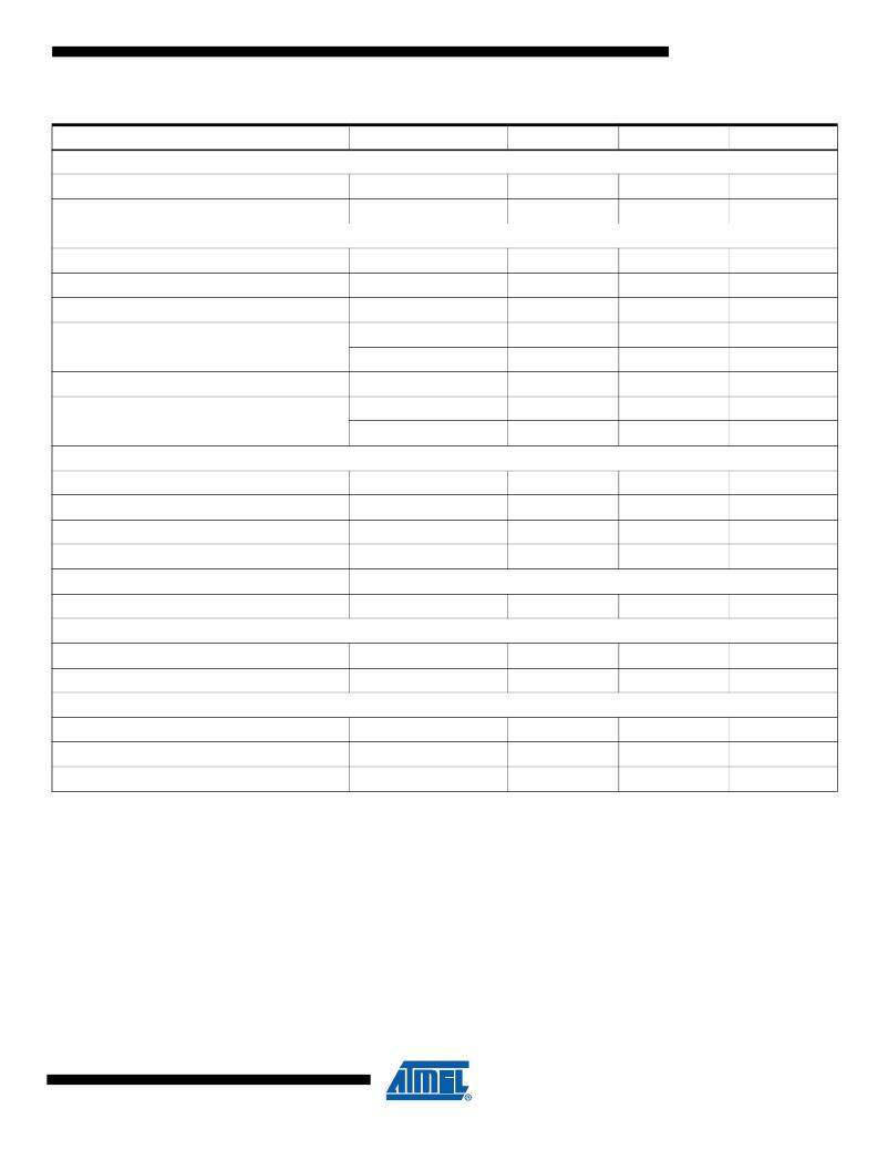
Table 6-1.
Command Listing
Command
Opcode
Address Bytes
Dummy Bytes
Data Bytes
Read Commands
Read Array
Read Array (Low Frequency)
0Bh
03h
0000 1011
0000 0011
3
3
1
0
1+
1+
Program and Erase Commands
Block Erase (4 Kbytes)
Block Erase (32 Kbytes)
Block Erase (64 Kbytes)
Chip Erase
Byte/Page Program (1 to 256 Bytes)
20h
52h
D8h
60h
C7h
02h
0010 0000
0101 0010
1101 1000
0110 0000
1100 0111
0000 0010
3
3
3
0
0
3
0
0
0
0
0
0
0
0
0
0
0
1+
Sequential Program Mode
ADh
AFh
1010 1101
1010 1111
3, 0
3, 0
(1)
(1)
0
0
1
1
Protection Commands
Write Enable
Write Disable
Protect Sector
Unprotect Sector
06h
04h
36h
39h
0000 0110
0000 0100
0011 0110
0011 1001
0
0
3
3
0
0
0
0
0
0
0
0
Global Protect/Unprotect
Use Write Status Register command
Read Sector Protection Registers
3Ch
0011 1100
3
0
1+
Status Register Commands
Read Status Register
Write Status Register
05h
01h
0000 0101
0000 0001
0
0
0
0
1+
1
Miscellaneous Commands
Read Manufacturer and Device ID
Deep Power-down
Resume from Deep Power-down
9Fh
B9h
ABh
1001 1111
1011 1001
1010 1011
0
0
0
0
0
0
1 to 4
0
0
Note:
1. Three address bytes are only required for the first operation to designate the address to start programming at. Afterwards,
the internal address counter automatically increments, so subsequent Sequential Program Mode operations only require
clocking in of the opcode and the data byte until the Sequential Program Mode has been exited.
7
3600G–DFLASH–06/09
发布紧急采购,3分钟左右您将得到回复。
相关PDF资料
AT26DF161-SU
IC FLASH 16MBIT 66MHZ 8SOIC
AT26DF161A-MU
IC FLASH 16MBIT 70MHZ 8QFN
AT26DF321-SU
IC FLASH 32MBIT 66MHZ 8SOIC
AT27BV010-90JU
IC OTP 1MBIT 90NS 32PLCC
AT27BV020-90JU
IC OTP 2MBIT 90NS 32PLCC
AT27BV040-12JU
IC OTP 4MBIT 120NS 32PLCC
AT27BV1024-90JU
IC OTP 1MBIT 90NS 44PLCC
AT27BV256-70JU
IC OTP 256KBIT 70NS 32PLCC
相关代理商/技术参数
AT26DF081A-SSU-RET
制造商:Atmel Corporation 功能描述:
AT26DF081A-ST-B
制造商:Adesto Technologies Corporation 功能描述:8-SOIC-W, AUTO GRADE 3, 2.7V, TUBE - Rail/Tube
AT26DF081A-ST-T
制造商:Adesto Technologies Corporation 功能描述:8-SOIC-W, AUTO GRADE 3, 2.7V, T&R - Tape and Reel
AT26DF081A-SU
功能描述:闪存 8M 8 I/O Pins SPI 256B 2.7V-3.6V RoHS:否 制造商:ON Semiconductor 数据总线宽度:1 bit 存储类型:Flash 存储容量:2 MB 结构:256 K x 8 定时类型: 接口类型:SPI 访问时间: 电源电压-最大:3.6 V 电源电压-最小:2.3 V 最大工作电流:15 mA 工作温度:- 40 C to + 85 C 安装风格:SMD/SMT 封装 / 箱体: 封装:Reel
AT26DF081-MU
制造商:Adesto Technologies Corporation 功能描述:SF DATAFLASH, 8M, MLF, IND TEMP,GREEN - Trays
AT26DF081-SU
制造商:Adesto Technologies Corporation 功能描述:SF DATAFLASH, 8M, SOIC ,IND TEMP, GREEN - Rail/Tube
AT26DF161
制造商:ATMEL 制造商全称:ATMEL Corporation 功能描述:16-megabit 2.7-volt Only Serial Firmware DataFlash Memory
AT26DF161_06
制造商:ATMEL 制造商全称:ATMEL Corporation 功能描述:16-megabit 2.7-volt Only Serial Firmware DataFlash Memory
